Del Mar Photonics - Newsletter Fall 2010 - Newsletter Winter 2010
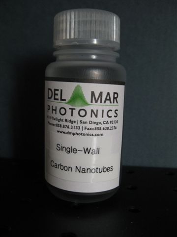
Single-Wall Carbon Nanotubes
Request specifications and quote
Featured Application
Saturable absorber relies on carbon nanotubes
John Wallace
A saturable absorber is a nonlinear optical material that becomes more
transparent as the intensity of light falling upon it increases. Passive
saturable absorbers can be integrated into laser systems to provide modelocking
and into fiberoptic systems for passive optical regeneration. The traditional
saturable absorber is a multiple-quantum-well (MQW) structure that requires
expensive equipment for fabrication—cleanroom-housed metal-oxide chemical-vapor
deposition or similar approaches to create the structure itself, and ion
implantation to reduce the device's saturation recovery time from the nanosecond
to the more practical picosecond range.
Researchers at Alnair Labs (Saitama-ken, Japan), the National Institute of
Advanced Industrial Science and Technology (Ibaraki, Japan), Tokyo Metropolitan
University (Tokyo, Japan), and the Research Center for Advanced Science and
Technology Tokyo, Japan) have created a saturable absorber from a layer of
single-walled carbon nanotubes sandwiched between two pieces of glass, termed a
saturable absorber incorporating nanotubes (SAINT). The fabrication process is
simple, consisting of spraying nanotubes onto glass. Because carbon nanotubes
are chemically stable, no hermetic sealing is required. The optical damage
threshold of the device is higher than that of a MQW saturable absorber; in
addition, a SAINT works in transmission—an easier-to-work-with mode of operation
than the reflective mode required for a MQW device.
The nanotubes themselves are synthesized by ablating a metal-catalyzed carbon
target with a Nd:YAG laser in 500 Torr of argon gas. The resulting tubes, with a
mean diameter of 1.1 nm, are dispersed in ethanol and sprayed onto 1-mm-thick
substrates with an airbrush (see figure). The researchers used the SAINTs for
two purposes: a noise-suppressing saturable absorber for 1550-nm light, and a
modelocked fiber laser operating in the same 1550-nm spectral region.
Single-walled carbon nanotubes are imaged by an atomic-force microscope (left)
and a transmission electron microscope (right). When sprayed onto a glass
substrate, these nanotubes exhibit saturable absorption of light, a property
useful in fiberoptic systems for noise suppression and laser modelocking.
Click here to enlarge image
The light source for the saturable-absorber setup was a fiber laser producing
1-ps pulse bunches (of about 120 pulses at a time) at an 80-GHz repetition rate.
A fiber collimator and an aspheric lens brought the light to a focus on the
SAINT. Varying the spot size by shifting the nanotube sample along the optical
axis varied the intensity of light falling on the carbon-nanotube film. At a
maximum peak intensity of 5.8 MW/cm2, the device reached a transmission of
almost 69%, whereas transmission dropped to about 63% at lower powers. Spectral
measurements indicate an inhomogeneously broadened absorption that responds on a
1-ps timescale. The performance of this first SAINT device is still far from its
full potential, the researchers note.
Two configurations
Modelocking a fiber laser is ordinarily done with a semiconductor saturable
absorber mirror (SESAM). For their modelocking experiment using a SAINT instead
of a SESAM, the researchers put together a fiber laser in two different
configurations, one with a ring geometry and the other of linear orientation.
The erbium-doped ring laser was backward pumped with a 980-nm laser diode, with
two optical isolators ensuring operation in one direction only. The SAINT and
associated optics were simply inserted in a break in the ring—a geometry
impossible with an ordinary reflective SESAM.
The ring laser began to modelock at a pump power of 18 mW, which could then be
backed off to 14 mW, with the laser operating at 6.1 MHz in single-pulse mode
(higher pump powers resulted in multiple-pulse operation at harmonics of 6.1
MHz). The resulting soliton pulses had a full-width half-maximum (FWHM) width of
1.1 ps, and were somewhat chirped—though the chirping could be reduced with the
use of low-dispersion fiber. When the SAINT was removed from the laser cavity,
all modelocking stopped, even at high pump powers.
The linear version of the modelocked fiber laser produced nonsoliton pulses at a
repetition rate of 9.85 MHz, a FWHM width of 318 fs, a 3-dB spectral width of
13.6 nm, and an average power of almost 1 mW. "We believe this is the first
demonstration of using carbon nanotubes for practical applications in the field
of applied optics," said Sze Set, general manager of research and development at
Alnair Labs, who noted that there was great interest in this material at this
year's Optical Fiber Communications Conference (Atlanta, GA; March 23–28).
Del Mar Photonics is involved in research of CNTs, graphene nanoplatelets and graphene materials, develops advanced multifunctional materials for variety of applications as well as research instrumentation for characterization of the above.
We currently we can offer:
1) Graphene nanoplatelets: the stack of multi-layer graphene sheets with high
aspect ratio, diameter: 0.5-20 µm,
thickness: 5-25 nm.
2) Graphene materials: Graphene Powder, Graphene Oxide Powder, Graphene
Suspension.
3) Carbon Nanotubes.
Contact our application team to discuss your requirements for high-performance nanocomposite materials, display materials, sensing materials, ultracapacitors, batteries, energy storage and other area to improve electrical, thermal, barrier, or mechanical properties by using low-cost nano-additive.
Graphene nanoplatelets are the stack of multi-layer graphene sheets including platelet morphology, with characteristics as follows:
| Physical Properties | |||||
| Diameter | Thickness | Specific Surface Area | Density | Electrical Conductivity | Tensile Strength |
| 0.5 - 20 µm | 5 - 25 nm | 40-60 m2/g | ~2.25 g/cm3 | 8000-10000 S/m | 5 GPa |
| Bulk Characteristics | ||||
| Appearance | Carbon content | Bulk density | Water Content | Residual impurities |
| A black and grey powder | >99.5% | ~0.30 g/ml | <0.5 wt% | <0.5 wt% |
Request a quote for graphene nanoplatelets
Applications:
The high performance composite additives in PPO, POM, PPS, PC, ABS,
PP, PE, PS, Nylon and rubbers.
To improve composite tensile strength, stiffness, corrosion resistance, abrasion
resistance and anti-static and lubricant properties.
Mechanical properties modifications.
Conductivity modification.
Fuel tank coating.
In electronic enclosures add electrical conductivity to polymers at low
densities of 3 to 5 wt%.
Adding EMI or RFI shielding capabilities to a variety of polymers.
Automotive parts: a composite with nanoplatelets can be painted
electrostatically, thereby saving costs.
Aerospace: graphite has long been used in aerospace composites. Nanoplatelets
can be combined with other additives to reinforce stiffness, add electrical
conductivity, EMI shielding, etc.
Appliances: fortified polymers provide superior thermal and electrical
conductivity, thereby saving the costs of separate heat dissipation mechanisms.
Sporting goods: graphite-based composites are stronger and stiffer and lighter
than comparable materials.
Coatings and paints: graphene nanoplatelets can be dispersed in a wide variety
of materials to add electrical conductivity and surface durability.
Batteries: graphene nanoplatelets increase the effectiveness of Lithium-ion
batteries when used to formulate electrodes.
Fuel cells: both bi-polar plate and electrode efficiencies can be improved.
Del Mar Photonics develops advanced instrumentation for research of CNTs, graphene nanoplatelets and graphene materials including lasers for broadband spectroscopy, femtosecond transient absorption and fluorescence measurements.
T&D Scan high
resolution Laser Spectrometer based on broadly tunable CW laser
CW single-frequency ring Dye laser
Beacon Femtosecond Optically Gated Fluorescence Kinetic Measurement System
New Hatteras femtosecond transient
absorption system
Photon Scanning Tunneling Microscope
Graphene is a one-atom-thick planar sheet of sp2-bonded carbon atoms that are
densely packed in a honeycomb crystal lattice. The term Graphene was coined as a
combination of graphite and the suffix -ene by Hanns-Peter Boehm,[1][2] who
described single-layer carbon foils in 1962.[3] Graphene is most easily
visualized as an atomic-scale chicken wire made of carbon atoms and their bonds.
The crystalline or "flake" form of graphite consists of many graphene sheets
stacked together.
The carbon-carbon bond length in graphene is about 0.142 nm. Graphene sheets
stack to form graphite with an interplanar spacing of 0.335 nm, which means that
a stack of 3 million sheets would be only one millimeter thick. Graphene is the
basic structural element of some carbon allotropes including graphite, charcoal,
carbon nanotubes, and fullerenes. It can also be considered as an indefinitely
large aromatic molecule, the limiting case of the family of flat polycyclic
aromatic hydrocarbons. The Nobel Prize in Physics for 2010 was awarded to Andre
Geim and Konstantin Novoselov "for groundbreaking experiments regarding the
two-dimensional material graphene".[4]
Graphene is a flat monolayer of carbon atoms tightly packed into a two-dimensional (2D) honeycomb lattice, and is a basic building block for graphitic materials of all other dimensionalities. It can be wrapped up into 0D fullerenes, rolled into 1D nanotubes or stacked into 3D graphite.[5]
References
[1] H. P. Boehm, R. Setton, E. Stumpp (1994). "Nomenclature and terminology of
graphite intercalation compounds". Pure and Applied Chemistry 66 (9): 1893–1901.
doi:10.1351/pac199466091893.
[2] H. C. Schniepp, J.-L. Li, M. J. McAllister, H. Sai, M. Herrera-Alonso, D. H.
Adamson, R. K. Prud’homme, R. Car, D. A. Saville, I. A. Aksay (2006).
"Functionalized Single Graphene Sheets Derived from Splitting Graphite Oxide".
The Journal of Physical Chemistry B 110 (17): 8535–8539. doi:10.1021/jp060936f.
PMID 16640401.
[3] H. P. Boehm, A. Clauss, G. O. Fischer, U. Hofmann (1962). "Das
Adsorptionsverhalten sehr dünner Kohlenstoffolien". Zeitschrift für anorganische
und allgemeine Chemie 316 (3-4): 119–127. doi:10.1002/zaac.19623160303.
[4] Nobel Foundation announcement
[5] Geim, A. K. and Novoselov, K. S. (2007). "The rise of
graphene". Nature Materials 6 (3): 183–191. doi:10.1038/nmat1849. PMID 17330084.
Carbon nanotubes (CNTs; also known as buckytubes) are allotropes of carbon
with a cylindrical nanostructure. Nanotubes have been constructed with
length-to-diameter ratio of up to 132,000,000:1,[1] which is significantly
larger than any other material. These cylindrical carbon molecules have novel
properties which make them potentially useful in many applications in
nanotechnology, electronics, optics, and other fields of materials science, as
well as potential uses in architectural fields. They may also have applications
in the construction of body armor. They exhibit extraordinary strength and
unique electrical properties, and are efficient thermal conductors.
Nanotubes are members of the fullerene structural family, which also includes
the spherical buckyballs. The ends of a nanotube may be capped with a hemisphere
of the buckyball structure. Their name is derived from their size, since the
diameter of a nanotube is on the order of a few nanometers (approximately
1/50,000th of the width of a human hair), while they can be up to 18 centimeters
in length (as of 2010).[1] Nanotubes are categorized as single-walled nanotubes
(SWNTs) and multi-walled nanotubes (MWNTs).
Chemical bonding in nanotubes is described by applied quantum chemistry,
specifically, orbital hybridization. The chemical bonding of nanotubes is
composed entirely of sp2 bonds, similar to those of graphite. These bonds, which
are stronger than the sp3 bonds found in diamonds, provide nanotubules with
their unique strength. Moreover, nanotubes naturally align themselves into
"ropes" held together by Van der Waals forces.
[1] Wang, X.; Li, Q.; Xie, J.; Jin, Z.; Wang, J.; Li, Y.; Jiang, K.; Fan, S. (2009). "Fabrication of Ultralong and Electrically Uniform Single-Walled Carbon Nanotubes on Clean Substrates". Nano Letters 9 (9): 3137–3141. doi:10.1021/nl901260b. PMID 19650638.
![]()
Del Mar Photonics, Inc.
4119 Twilight Ridge
San Diego, CA 92130
tel: (858) 876-3133
fax: (858) 630-2376
Skype: delmarphotonics
sales@dmphotonics.com
If you have trouble navigating our website, just
send us a quick e-mail and we'll be happy to answer all your questions!
![]()
![]()
![]()
![]()